THREE TERMINAL VOLTAGE REGULATOR
These voltage regulators are monolithic integrated circuits designed as
fixed–voltage regulators for a wide variety of applications including local,
on–card regulation. These regulators employ internal current limiting,
thermal shutdown, and safe–area compensation. With adequate heatsinking
they can deliver output currents in excess of 1.0 A. Although designed
primarily as a fixed voltage regulator, these devices can be used with
external components to obtain adjustable voltages and currents.
• Output Current in Excess of 1.0 A
• No External Components Required
• Internal Thermal Overload Protection
• Internal Short Circuit Current Limiting
• Output Transistor Safe–Area Compensation
• Output Voltage Offered in 2% and 4% Tolerance
• Available in Surface Mount D2PAK and Standard 3–Lead Transistor
Packages


The centre region is called the base and gains its name from the fact that in the very earliest transistors it formed the "base" for the whole structure. The other two connections are called the emitter and collector. These names result from the way in which they either emit or collect the charge carriers. It is also essential that the base region is very thin if the device is to be able to operate. In today's transistors the base may typically be only about 1 mm [micrometre] across. It is the fact that the base region of the transistor is thin that is the key to the operation of the device
For clarity the example of an NPN transistor is taken. The same reasoning can be used for a PNP device, except that holes are the majority carriers instead of electrons.
When current flows through the base emitter junction, electrons leave the emitter and flow into the base. However the doping in this region is kept low and there are comparatively few holes available for recombination. As a result most of the electrons are able to flow right through the base region and on into the collector region, attracted by the positive potential.

Only a small proportion of the electrons from the emitter combine with holes in the base region giving rise to a current in the base-emitter circuit. This means that the collector current is much higher. The ratio between the collector current and the base current is given the Greek symbol b. For most small signal transistors this may be in the region 50 to 500. In some cases it can be even higher. This means that the collector current is typically between 50 and 500 times that flowing in the base. For a high power transistor the value of b is somewhat less: 20 is a fairly typical value.
For example, a capacitor can be labelled as, n47 = 0.47nF, 4n7 = 4.7nF or 47n = 47nF and so on. Also, sometimes capacitors are marked with the capital letter K to signify a value of one thousand pico-Farads, so for example, a capacitor with the markings of 100K would be 100 x 1000pF or100nF.
To reduce the confusion regarding letters, numbers and decimal points, an International colour coding scheme was developed many years ago as a simple way of identifying capacitor values and tolerances. It consists of coloured bands (in spectral order) known commonly as the Capacitor Colour Code system and whose meanings are illustrated below:
An example of the use of capacitor colour codes is given as:
The Capacitor Colour Code system was used for many years on unpolarised polyester and mica moulded capacitors. This system of colour coding is now obsolete but there are still many "old" capacitors around. Nowadays, small capacitors such as film or disk types conform to the BS1852 Standard and its new replacement, BS EN 60062, were the colours have been replaced by a letter or number coded system.
Generally the code consists of 2 or 3 numbers and an optional tolerance letter code to identify the tolerance. Where a two number code is used the value of the capacitor only is given in picofarads, for example, 47 = 47 pF and 100 = 100pF etc. A three letter code consists of the two value digits and a multiplier much like the resistor colour codes in the resistors section.
For example, the digits 471 = 47*10 = 470pF. Three digit codes are often accompanied by an additional tolerance letter code as given below.
Consider the capacitor below:

Then by just using numbers and letters as codes on the body of the capacitor we can easily determine the value of its capacitance either in Pico-farad's, Nano-farads or Micro-farads and a list of these "international" codes is given in the following table along with their equivalent capacitances.
There are many different types of diodes that are available for use in electronics design.
Different semiconductor diode types can be used to perform different functions as a result of the properties of these different diode types.
Semiconductor diodes can be used for many applications. The basic application is obviously to rectify waveforms. This can be used within power supplies or within radio detectors. Signal diodes can also be used for many other functions within circuits where the "one way" effect of a diode may be required.

Leaded Semiconductor Diodes
Diodes are not just used as rectifiers, as various other types of diode can be used in many other applications. Some other different types of diodes include: light emitting diodes, photo-diodes, laser diodes and more as detailed in the list below.
Many of the different types of diodes mentioned below have further pages providing in-depth information about them including their structures, method of operation, how they may be used in circuits, and precautions and tips for using them in electronics design.
Semiconductor diodes are widely used throughout all areas of the electronics industry from electronics design through to production and repair. The semiconductor diode is very versatile, and there are very many variants and different types of diode that enable all the variety of different applications to be met.
The different diode types of types of diodes include those for small signal applications, high current and voltage as well as different types of diodes for light emission and detection as well as types for low forward voltage drops, and types to give variable capacitance. In addition to this there are a number of diode types that are used for microwave applications.
THE DIODE SYMBOL
The diode symbol is very similar to an arrow touching a "bar". The "bar" is the cathode and this is the end we refer to when describing a diode.

TYPES OF DIODE There are three main types of diodes:
1. The signal diode (ordinary diode)
2. The power diode, (ordinary diode) and
3. The zener diode . . . plus lots of specialized types.
The Zener diode is covered separately.
In this section we will cover the "ordinary" diode.
DIODE OPERATION
The ordinary diode has a single feature. It only allows current to flow in one direction. This is called the forward-bias direction, when the voltage on the anode is higher than the cathode. The flow of current is in the direction of the arrow on the symbol.
When the diode is in the reverse-bias direction (when a high voltage is connected to the cathode lead and the anode is connected to the 0v rail) the diode exhibits a very high resistance and no current flows.
The diagram below shows the diode in forward-bias:

No current flows through the diode until 0.7v is on the anode and any voltage above 0.7v appears on the other end of the diode. Thus we say the diode has a 0.7v drop across it and this voltage does not change from one diode to another or due to the current flowing. (We are discussing silicon diodes. Germanium diodes have 0.2v across them and Schottky diodes have 0.3 to 0.4v across them).
If the diode is reversed, it will be in reverse-bias mode and no current will flow. This is shown in the diagram below:

Note: The supply is on the right-hand-side of the circuit - this is the normal way a power supply is drawn - and the arrow on the diode is "opposing" the flow of current.
TESTING A DIODEDiodes can be tested with a multimeter set to HIGH OHMS range.
Inside the multimeter is a battery (1.5v or 3v) and this provides the energy to move the needle. One very important point to note is the red probe of a multimeter is connected to negative of the battery (inside the multimeter) and the black probe is connected to the positive of the battery (via a set of resistors and the meter-movement itself).
When the black probe is connected to the anode of a diode and the red probe to the cathode, as shown in the animation below, the needle moves about 90% across the dial. (It does not move fully across because the multimeter is actually detecting the voltage-drop of 0.7v of the diode and not its actual resistance - but this is a technical point).
When the red probe is connected to the anode and the black probe to the cathode, the needle does not move at all.
In the first case the diode is forward biased and current flows. In the second case the diode isreverse biased and no current flows. The pointer (needle) clearly indicates these two states. These are the two conditions we need to remember.
 FAULTS
If the needle does not move in either test, the diode is faulty - OPEN!
If the needle moves slightly in the reverse-bias test, the diode is LEAKY and should not be used.
If the needle moves fully across the dial, the diode is faulty - SHORTED!HOW A DIODE WORKS IN A CIRCUIT
Even though a diode performs only one action (to allow current to flow in only one direction), the surrounding components in a circuit will create a lot of different effects.
The simplest use for a diode is to convert AC to DC. AC is the name we give to a waveform that rises and falls in a smooth action. (Its technical name is Alternating Current but we also refer to AC as an alternating voltage). DC means Direct Current and this is the type of waveform obtained from a battery. We also refer to a fixed voltage as DC. In the diagram below we see the AC voltage rising and falling. AC is the type of voltage we get from the "mains."
 An example of "AC" and "DC"
When we put a transformer on the mains, we can obtain an AC voltage, that has the same shape as the 120v or 240v "mains," but a lower value. In the diagram below one line of the secondary of a transformer is connected to the 0v rail of a project and the other line rises 9v above and 9v below the 0v rail as shown in the animation below. The 0v rail is also called "earth."
An example of "AC" and "DC"
When we put a transformer on the mains, we can obtain an AC voltage, that has the same shape as the 120v or 240v "mains," but a lower value. In the diagram below one line of the secondary of a transformer is connected to the 0v rail of a project and the other line rises 9v above and 9v below the 0v rail as shown in the animation below. The 0v rail is also called "earth."

If we connect a diode to the line that rises and falls, the output of the diode will only contain the positive portion of the waveform, as shown in the animation below. This is because the diode only allows voltage above 0.7v to pass through it.

This process is called RECTIFICATION and the output of the diode consists of only the positive portion of the waveform as shown below:

By adding an electrolytic to the output of the diode, the positive pulses will be turned into a smooth voltage of approx 9v - 0.7v = 8.3v The electrolytic charges up during the first pulse and it stores the voltage so that the waveform does not fall. This is shown in the diagram below:

If current is delivered by the circuit above, the energy (current) is taken from the electrolytic and the voltage across it drops slightly until it is charged again by the diode in the next cycle.
The circuit above is called a half-wave rectifier as only the positive portions of the waveform are delivered to the output.
An improved design is called a FULL-WAVE rectifier and both the positive and negative portions of the waveform are delivered to the output.
This requires 4 diodes in a BRIDGE arrangement as shown below.

The layout of the 4 diodes (the bridge) is very easy to remember as each diode faces in the direction of the flow of energy, and so a single diode can be shown for the bridge, as shown below:

The animation below shows that only two diodes at a time transfer energy. Two diodes transfer the positive portion of the waveform then the other two diodes deliver the negative portion of the wave. Watch the output voltage rise and fall as the voltage is traced out on the sinewave. Note how the diodes change from one set to the other as the AC voltage changes from one direction to the other.

The result is the output consists of peaks that are closely spaced and the job of smoothing out these peaks is done by an electrolytic.
THE DIODE AS A LIMITER
A diode can be used to limit the amplitude of a signal, as shown in the diagram below. Since a diode does not turn on until 0.7v, any signal below this value will pass from the left-hand-side of the circuit to the right side. Any waveform above 0.7v will be "clipped" or "limited" by the diode and this will cause "distortion". This distortion may be wanted, such as "FUZZ" in a guitar amplifier. The diode also has the effect of converting sinewave signals into a square wave.

THE DIODE AS A PROTECTOR
The diode can be used to protect a project from reverse-voltage and over-voltage. Here are 3 arrangements.
1. A project can be protected from reverse voltage by placing a diode on the positive input line. The diode must be capable of handing the input current. The only disadvantage of this design is the 0.7v drop across the diode.
 Adding a diode to the input line
2. If the project is operating from a 12v car battery, for example, the 0.7v loss can be overcome by placing a zener across the input as shown below.
Adding a diode to the input line
2. If the project is operating from a 12v car battery, for example, the 0.7v loss can be overcome by placing a zener across the input as shown below.
The zener must be a high current type as a reverse voltage or over-voltage will cause the zener to conduct and the high current is designed to blow the fuse.
 Connecting a zener across the input
3. If you only require reverse-voltage protection, a diode can be placed across the input as shown below. The diode must be a power diode such as 1N 5404.
Connecting a zener across the input
3. If you only require reverse-voltage protection, a diode can be placed across the input as shown below. The diode must be a power diode such as 1N 5404.

If you want to be able to power a project via a DC voltage that is connected EITHER WAY! you can use the very clever circuit below. The only disadvantage is a loss of 1.2v across the two diodes that come into operation when the DC voltage is applied.

If you want to power a 5v microprocessor project from a 6v battery (such as a lantern battery or 4 AA cells), a diode can be placed in the positive line to drop 0.7v. The remaining 5.3v is an ideal voltage for a micro project. The diode also serves to prevent reverse-polarity connection.

THE DIODE BRIDGE
Many projects use 4 diodes in a bridge arrangement in the power supply and if the current requirement is fairly high, (1 amp or more) one or more of the diodes can go open and create an unusual fault. In many cases, the power supply will contain a 50Hz/60Hz or 100Hz hum. If the diodes are separate, check the temperature of each diode with a finger. If one diode is getting VERY hot, its equivalent on the other side of the bridge is open.
If the fault has occurred in an encapsulated bridge module, place a diode across each of the diodes in turn and hold the diode in your fingers. If it gets warm, the diode in the bridge has gone open.
Bridge modules are sometimes hard to identify. The diagrams below show some of the identifications. They are: surface-mount type, W04 (1.5amp bridge), bridge in a chip, and 10amp to 50 amp bridge.

IN-CIRCUIT TESTING
A diode can be tested in-circuit with a multimeter but the reading may be affected by the surrounding components. Lift one end out of circuit to prevent false readings.
fixed–voltage regulators for a wide variety of applications including local,
on–card regulation. These regulators employ internal current limiting,
thermal shutdown, and safe–area compensation. With adequate heatsinking
they can deliver output currents in excess of 1.0 A. Although designed
primarily as a fixed voltage regulator, these devices can be used with
external components to obtain adjustable voltages and currents.
• Output Current in Excess of 1.0 A
• No External Components Required
• Internal Thermal Overload Protection
• Internal Short Circuit Current Limiting
• Output Transistor Safe–Area Compensation
• Output Voltage Offered in 2% and 4% Tolerance
• Available in Surface Mount D2PAK and Standard 3–Lead Transistor
Packages
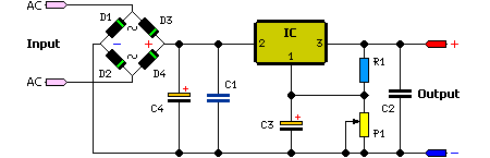
BASIC ELECTRONICS REGULATED POWER SUPPLIES
Unfortunately our hobby circuit work on different voltages and a power supply with single voltage will not be sufficient. Simplest way would be to buy a multi-tapped transformer and connect the voltage taps with a suitable switch. These transformers are available with taps of 1.5, 3, 4.5, 6, 9, 12v. We need a single multi throw switch ( as many throws as there are taps). With 9-6-0-6-9 transformer and with a double pole double throw switch, you can get 6 and 9V dc. With the same transformer , and with a double pole double throw switch it is possible to get 3, 6, 9, 12, 15, 18V. Switches and multi – taped transformers are difficult to procure; cumbersome and even unavailable at some places.
Such schematics are not shown here as there are better way to build circuits to get variable voltages. Also these power supplies suffer from a major draw back ; poor valtage regulation, voltage fluctuations.
A12V power supply shown in schematic 3 may show as much as 16.8V without load and it may go down to less than 12V as the load current is increased. This still can be and is safely circuits, we will user them for the pleasure and ease of using them and build regulated power supply as a starter.
We have some wonderful devices in three terminal regulators, just three terminals, IN- GROUND – OUT
BASIC ELECTRONICS IC
INTIGRATED CIRCUIT ( IC )
Intigrated Circuit actually consist of a number of active electronic components such as transistors and diodes along with other passive components such as resistors and capacitors interconnected as a single unit on semi conducting wafer usually silicon. Integrated circuits are classified as analog, digital and mixed signal (both analog and digital on the same chip).
BASIC ELECTRONICS TRANSISTOR
Basic transistor structure
The transistor is a three terminal device and consists of three distinct layers. Two of them are doped to give one type of semiconductor and the there is the opposite type, i.e. two may be n-type and one p-type, or two may be p-type and one may be n-type.. They are arranged so that the two similar layers of the transistor sandwich the layer of the opposite type. As a result transistor are designated either P-N-P (PNP) types of N-P-N (NPN) types according to the way they are made up.Transistor operation
A transistor can be considered as two P-N junctions placed back to back. One of these, namely the base emitter junction is forward biased, whilst the other, the base collector junction is reverse biased. It is found that when a current is made to flow in the base emitter junction a larger current flows in the collector circuit even though the base collector junction is reverse biased.For clarity the example of an NPN transistor is taken. The same reasoning can be used for a PNP device, except that holes are the majority carriers instead of electrons.
When current flows through the base emitter junction, electrons leave the emitter and flow into the base. However the doping in this region is kept low and there are comparatively few holes available for recombination. As a result most of the electrons are able to flow right through the base region and on into the collector region, attracted by the positive potential.
BASIC ELECTRONICS CAPACITOR
Capacitor Colour Codes
Generally, the actual values of Capacitance, Voltage or Tolerance are marked onto the body of the capacitors in the form of alphanumeric characters. However, when the value of the capacitance is of a decimal value problems arise with the marking of a "Decimal Point" as it could easily not be noticed resulting in a misreading of the actual value. Instead letters such as p (pico) or n (nano) are used in place of the decimal point to identify its position and the weight of the number.For example, a capacitor can be labelled as, n47 = 0.47nF, 4n7 = 4.7nF or 47n = 47nF and so on. Also, sometimes capacitors are marked with the capital letter K to signify a value of one thousand pico-Farads, so for example, a capacitor with the markings of 100K would be 100 x 1000pF or100nF.
To reduce the confusion regarding letters, numbers and decimal points, an International colour coding scheme was developed many years ago as a simple way of identifying capacitor values and tolerances. It consists of coloured bands (in spectral order) known commonly as the Capacitor Colour Code system and whose meanings are illustrated below:
Capacitor Colour Code Table
Colour
|
Digit
A |
Digit
B |
Multiplier
D |
Tolerance
(T) > 10pf |
Tolerance
(T) < 10pf |
Temperature Coefficient
(TC) |
Black
|
0
|
0
|
x1
|
± 20%
|
± 2.0pF
| |
Brown
|
1
|
1
|
x10
|
± 1%
|
± 0.1pF
|
-33x10-6
|
Red
|
2
|
2
|
x100
|
± 2%
|
± 0.25pF
|
-75x10-6
|
Orange
|
3
|
3
|
x1,000
|
± 3%
|
-150x10-6
| |
Yellow
|
4
|
4
|
x10,000
|
± 4%
|
-220x10-6
| |
Green
|
5
|
5
|
x100,000
|
± 5%
|
± 0.5pF
|
-330x10-6
|
Blue
|
6
|
6
|
x1,000,000
|
-470x10-6
| ||
Violet
|
7
|
7
|
-750x10-6
| |||
Grey
|
8
|
8
|
x0.01
|
+80%,-20%
| ||
White
|
9
|
9
|
x0.1
|
± 10%
|
± 1.0pF
| |
Gold
|
x0.1
|
± 5%
| ||||
Silver
|
x0.01
|
± 10%
|
Capacitor Voltage Colour Code Table
Colour
|
Voltage Rating (V)
| ||||
Type J
|
Type K
|
Type L
|
Type M
|
Type N
| |
Black
|
4
|
100
|
10
|
10
| |
Brown
|
6
|
200
|
100
|
1.6
| |
Red
|
10
|
300
|
250
|
4
|
35
|
Orange
|
15
|
400
|
40
| ||
Yellow
|
20
|
500
|
400
|
6.3
|
6
|
Green
|
25
|
600
|
16
|
15
| |
Blue
|
35
|
700
|
630
|
20
| |
Violet
|
50
|
800
| |||
Grey
|
900
|
25
|
25
| ||
White
|
3
|
1000
|
2.5
|
3
| |
Gold
|
2000
| ||||
Silver
| |||||
Capacitor Voltage Reference
- Type J - Dipped Tantalum Capacitors.
- Type K - Mica Capacitors.
- Type L - Polyester/Polystyrene Capacitors.
- Type M - Electrolytic 4 Band Capacitors.
- Type N - Electrolytic 3 Band Capacitors.
An example of the use of capacitor colour codes is given as:
Metalised Polyester Capacitor
 |
Disc & Ceramic Capacitor
 |
The Capacitor Colour Code system was used for many years on unpolarised polyester and mica moulded capacitors. This system of colour coding is now obsolete but there are still many "old" capacitors around. Nowadays, small capacitors such as film or disk types conform to the BS1852 Standard and its new replacement, BS EN 60062, were the colours have been replaced by a letter or number coded system.
Generally the code consists of 2 or 3 numbers and an optional tolerance letter code to identify the tolerance. Where a two number code is used the value of the capacitor only is given in picofarads, for example, 47 = 47 pF and 100 = 100pF etc. A three letter code consists of the two value digits and a multiplier much like the resistor colour codes in the resistors section.
For example, the digits 471 = 47*10 = 470pF. Three digit codes are often accompanied by an additional tolerance letter code as given below.
Capacitor Tolerance Letter Codes Table
Letter
|
B
|
C
|
D
|
F
|
G
|
J
|
K
|
M
|
Z
| |
Tolerance
|
C <10pF ±pF
|
0.1
|
0.25
|
0.5
|
1
|
2
| ||||
C >10pF ±%
|
0.5
|
1
|
2
|
5
|
10
|
20
|
+80-20
|
The capacitor on the left is of a ceramic disc type capacitor that has the code 473J printed onto its body. Then the 4 = 1st digit, the 7 = 2nd digit,
the 3 is the multiplier in pico-Farads, pF and the letter J is the tolerance and this translates to: 47pF * 1,000 (3 zero's) = 47,000 pF , 47nF or 0.047 uF the J indicates a tolerance of +/- 5% |
Capacitor Letter Codes Table
Picofarad
(pF) |
Nanofarad
(nF) |
Microfarad
(uF) |
Code
|
Picofarad
(pF) |
Nanofarad
(nF) |
Microfarad
(uF) |
Code
|
10
|
0.01
|
0.00001
|
100
|
4700
|
4.7
|
0.0047
|
472
|
15
|
0.015
|
0.000015
|
150
|
5000
|
5.0
|
0.005
|
502
|
22
|
0.022
|
0.000022
|
220
|
5600
|
5.6
|
0.0056
|
562
|
33
|
0.033
|
0.000033
|
330
|
6800
|
6.8
|
0.0068
|
682
|
47
|
0.047
|
0.000047
|
470
|
10000
|
10
|
0.01
|
103
|
100
|
0.1
|
0.0001
|
101
|
15000
|
15
|
0.015
|
153
|
120
|
0.12
|
0.00012
|
121
|
22000
|
22
|
0.022
|
223
|
130
|
0.13
|
0.00013
|
131
|
33000
|
33
|
0.033
|
333
|
150
|
0.15
|
0.00015
|
151
|
47000
|
47
|
0.047
|
473
|
180
|
0.18
|
0.00018
|
181
|
68000
|
68
|
0.068
|
683
|
220
|
0.22
|
0.00022
|
221
|
100000
|
100
|
0.1
|
104
|
330
|
0.33
|
0.00033
|
331
|
150000
|
150
|
0.15
|
154
|
470
|
0.47
|
0.00047
|
471
|
200000
|
200
|
0.2
|
254
|
560
|
0.56
|
0.00056
|
561
|
220000
|
220
|
0.22
|
224
|
680
|
0.68
|
0.00068
|
681
|
330000
|
330
|
0.33
|
334
|
750
|
0.75
|
0.00075
|
751
|
470000
|
470
|
0.47
|
474
|
820
|
0.82
|
0.00082
|
821
|
680000
|
680
|
0.68
|
684
|
1000
|
1.0
|
0.001
|
102
|
1000000
|
1000
|
1.0
|
105
|
1500
|
1.5
|
0.0015
|
152
|
1500000
|
1500
|
1.5
|
155
|
2000
|
2.0
|
0.002
|
202
|
2000000
|
2000
|
2.0
|
205
|
2200
|
2.2
|
0.0022
|
222
|
2200000
|
2200
|
2.2
|
225
|
3300
|
3.3
|
0.0033
|
332
|
3300000
|
3300
|
3.3
|
335
|
BASIC ELECTRONICS DIODE
DIODE
Different semiconductor diode types can be used to perform different functions as a result of the properties of these different diode types.
Semiconductor diodes can be used for many applications. The basic application is obviously to rectify waveforms. This can be used within power supplies or within radio detectors. Signal diodes can also be used for many other functions within circuits where the "one way" effect of a diode may be required.
Leaded Semiconductor Diodes
Many of the different types of diodes mentioned below have further pages providing in-depth information about them including their structures, method of operation, how they may be used in circuits, and precautions and tips for using them in electronics design.
Types of diodes
It is sometimes useful to summarise the different types of diode that are available. Some of the categories may overlap, but the various definitions may help to narrow the field down and provide an overview of the different diode types that are available.- Backward diode: This type of diode is sometimes also called the back diode. Although not widely used, it is a form of PN junction diode that is very similar to the tunnel diode in its operation. It finds a few specialist applications where its particular properties can be used.
- BARITT diode: This form of diode gains its name from the words Barrier Injection Transit Time diode. It is used in microwave applications and bears many similarities to the more widely used IMPATT diode.
- Gunn Diode: Although not a diode in the form of a PN junction, this type of diode is a semiconductor device that has two terminals. It is generally used for generating microwave signals.
- Laser diode: This type of diode is not the same as the ordinary light emitting diode because it produces coherent light. Laser diodes are widely used in many applications from DVD and CD drives to laser light pointers for presentations. Although laser diodes are much cheaper than other forms of laser generator, they are considerably more expensive than LEDs. They also have a limited life.
- Light emitting diodes: The light emitting diode or LED is one of the most popular types of diode. When forward biased with current flowing through the junction, light is produced. The diodes use component semiconductors, and can produce a variety of colours, although the original colour was red. There are also very many new LED developments that are changing the way displays can be used and manufactured. High output LEDs and OLEDs are two examples
- Photodiode: The photo-diode is used for detecting light. It is found that when light strikes a PN junction it can create electrons and holes. Typically photo-diodes are operated under reverse bias conditions where even small amounts of current flow resulting from the light can be easily detected. Photo-diodes can also be used to generate electricity. For some applications, PIN diodes work very well as photodetectors.
- PIN diode: This type of diode is typified by its construction. It has the standard P type and N-type areas, but between them there is an area of Intrinsic semiconductor which has no doping. The area of the intrinsic semiconductor has the effect of increasing the area of the depletion region which can be useful for switching applications as well as for use in photodiodes, etc.
- PN Junction: The standard PN junction may be thought of as the normal or standard type of diode in use today. These diodes can come as small signal types for use in radio frequency, or other low current applications which may be termed as signal diodes. Other types may be intended for high current and high voltage applications and are normally termed rectifier diodes.
- Schottky diodes: This type of diode has a lower forward voltage drop than ordinary silicon PN junction diodes. At low currents the drop may be somewhere between 0.15 and 0.4 volts as opposed to 0.6 volts for a silicon diode. To achieve this performance they are constructed in a different way to normal diodes having a metal to semiconductor contact. They are widely used as clamping diodes, in RF applications, and also for rectifier applications
- Step recovery diode: A form of microwave diode used for generating and shaping pulses at very high frequencies. These diodes rely on a very fast turn off characteristic of the diode for their operation.
- Tunnel diode: Although not widely used today, the tunnel diode was used for microwave applications where its performance exceeded that of other devices of the day.
- Varactor diode or varicap diode: This type of diode is used in many radio frequency (RF) applications. The diode has a reverse bias placed upon it and this varies the width of the depletion layer according to the voltage placed across the diode. In this configuration the varactor or varicap diode acts like a capacitor with the depletion region being the insulating dielectric and the capacitor plates formed by the extent of the conduction regions. The capacitance can be varied by changing the bias on the diode as this will vary the width of the depletion region which will accordingly change the capacitance.
- Zener diode: The Zener diode is a very useful type of diode as it provides a stable reference voltage. As a result it is used in vast quantities. It is run under reverse bias conditions and it is found that when a certain voltage is reached it breaks down. If the current is limited through a resistor, it enables a stable voltage to be produced. This type of diode is therefore widely used to provide a reference voltage in power supplies. Two types of reverse breakdown are apparent in these diodes: Zener breakdown and Impact Ionisation. However the name Zener diode is used for the reference diodes regardless of the form of breakdown that is employed.
The different diode types of types of diodes include those for small signal applications, high current and voltage as well as different types of diodes for light emission and detection as well as types for low forward voltage drops, and types to give variable capacitance. In addition to this there are a number of diode types that are used for microwave applications.
THE DIODE SYMBOL
The diode symbol is very similar to an arrow touching a "bar". The "bar" is the cathode and this is the end we refer to when describing a diode.
1. The signal diode (ordinary diode)
2. The power diode, (ordinary diode) and
3. The zener diode . . . plus lots of specialized types.
The Zener diode is covered separately.
In this section we will cover the "ordinary" diode.
DIODE OPERATION
The ordinary diode has a single feature. It only allows current to flow in one direction. This is called the forward-bias direction, when the voltage on the anode is higher than the cathode. The flow of current is in the direction of the arrow on the symbol.
When the diode is in the reverse-bias direction (when a high voltage is connected to the cathode lead and the anode is connected to the 0v rail) the diode exhibits a very high resistance and no current flows.
The diagram below shows the diode in forward-bias:
If the diode is reversed, it will be in reverse-bias mode and no current will flow. This is shown in the diagram below:
TESTING A DIODEDiodes can be tested with a multimeter set to HIGH OHMS range.
Inside the multimeter is a battery (1.5v or 3v) and this provides the energy to move the needle. One very important point to note is the red probe of a multimeter is connected to negative of the battery (inside the multimeter) and the black probe is connected to the positive of the battery (via a set of resistors and the meter-movement itself).
When the black probe is connected to the anode of a diode and the red probe to the cathode, as shown in the animation below, the needle moves about 90% across the dial. (It does not move fully across because the multimeter is actually detecting the voltage-drop of 0.7v of the diode and not its actual resistance - but this is a technical point).
When the red probe is connected to the anode and the black probe to the cathode, the needle does not move at all.
In the first case the diode is forward biased and current flows. In the second case the diode isreverse biased and no current flows. The pointer (needle) clearly indicates these two states. These are the two conditions we need to remember.
If the needle does not move in either test, the diode is faulty - OPEN!
If the needle moves slightly in the reverse-bias test, the diode is LEAKY and should not be used.
If the needle moves fully across the dial, the diode is faulty - SHORTED!HOW A DIODE WORKS IN A CIRCUIT
Even though a diode performs only one action (to allow current to flow in only one direction), the surrounding components in a circuit will create a lot of different effects.
The simplest use for a diode is to convert AC to DC. AC is the name we give to a waveform that rises and falls in a smooth action. (Its technical name is Alternating Current but we also refer to AC as an alternating voltage). DC means Direct Current and this is the type of waveform obtained from a battery. We also refer to a fixed voltage as DC. In the diagram below we see the AC voltage rising and falling. AC is the type of voltage we get from the "mains."
An example of "AC" and "DC" The circuit above is called a half-wave rectifier as only the positive portions of the waveform are delivered to the output.
An improved design is called a FULL-WAVE rectifier and both the positive and negative portions of the waveform are delivered to the output.
This requires 4 diodes in a BRIDGE arrangement as shown below.
THE DIODE AS A LIMITER
A diode can be used to limit the amplitude of a signal, as shown in the diagram below. Since a diode does not turn on until 0.7v, any signal below this value will pass from the left-hand-side of the circuit to the right side. Any waveform above 0.7v will be "clipped" or "limited" by the diode and this will cause "distortion". This distortion may be wanted, such as "FUZZ" in a guitar amplifier. The diode also has the effect of converting sinewave signals into a square wave.
The diode can be used to protect a project from reverse-voltage and over-voltage. Here are 3 arrangements.
1. A project can be protected from reverse voltage by placing a diode on the positive input line. The diode must be capable of handing the input current. The only disadvantage of this design is the 0.7v drop across the diode.
Adding a diode to the input lineThe zener must be a high current type as a reverse voltage or over-voltage will cause the zener to conduct and the high current is designed to blow the fuse.
Connecting a zener across the input Many projects use 4 diodes in a bridge arrangement in the power supply and if the current requirement is fairly high, (1 amp or more) one or more of the diodes can go open and create an unusual fault. In many cases, the power supply will contain a 50Hz/60Hz or 100Hz hum. If the diodes are separate, check the temperature of each diode with a finger. If one diode is getting VERY hot, its equivalent on the other side of the bridge is open.
If the fault has occurred in an encapsulated bridge module, place a diode across each of the diodes in turn and hold the diode in your fingers. If it gets warm, the diode in the bridge has gone open.
Bridge modules are sometimes hard to identify. The diagrams below show some of the identifications. They are: surface-mount type, W04 (1.5amp bridge), bridge in a chip, and 10amp to 50 amp bridge.
A diode can be tested in-circuit with a multimeter but the reading may be affected by the surrounding components. Lift one end out of circuit to prevent false readings.